Table of Contents
- Overview
- 1. Foundations of Sequential Circuits
- 2. SR Latches (Set-Reset)
- Delay)
- 4. Edge-Triggered D Flip-Flops
- 5. T Flip-Flops (Toggle)
- 5.1 Concept & Circuit Realization
- 5.2 Truth Table & State Analysis
- 5.3 Characteristic Equation & Excitation Table
- [[Sequential Circuits#54-frequency-division-property-f_out—f_in—2|5.4 Frequency Division Property ()]]
- 6. JK Flip-Flops & Race-Around Condition
- 7. Master-Slave Flip-Flops
- 8. Roadmap & Future Expansion (Registers & Counters)
- 9. GATE PYQ-Style Solved Questions
Unlike memoryless combinational circuits whose outputs depend solely on present inputs, sequential circuits contain memory elements (such as latches or flip-flops) and feedback paths. Their present output depends on both present inputs and the present state (past history) stored in memory.
In this note, we cover the foundational principles of sequential logic, level vs. edge triggering, and a comprehensive analysis of SR NOR, SR NAND, and D Latches.
1. Foundations of Sequential Circuits
1.1 Combinational vs. Sequential Logic
| Property | Combinational Circuits | Sequential Circuits |
|---|---|---|
| Output Dependency | Present inputs only | Present inputs + Present state () |
| Memory Element | Not required | Required (Latches / Flip-Flops) |
| Feedback Path | No feedback loop | Mandatory feedback loop |
| Clock Signal | Not required | Clock used in synchronous circuits |
| Examples | Adders, MUX, Decoders | Latches, Flip-Flops, Counters, Registers |
1.2 Level Triggering vs. Edge Triggering
Control signals (clock or enable ) dictate when a memory element updates its state:
-
Level Triggered (Latches):
- The circuit responds and changes state continuously as long as the control signal is held at a specific voltage level (High level or Low level ).
- Transparent Mode: While , any change at the data inputs immediately propagates to the output.
-
Edge Triggered (Flip-Flops):
- The circuit responds and samples inputs only during the transition (edge) of the clock pulse:
- Positive / Rising Edge (): Transition from .
- Negative / Falling Edge (): Transition from .
- Inputs are ignored during the rest of the clock cycle when the clock is steady high or low.
- The circuit responds and samples inputs only during the transition (edge) of the clock pulse:
1.3 Latches vs. Flip-Flops
- Latch: A level-sensitive bistable memory element without a clock or operated via a level enable.
- Flip-Flop: An edge-sensitive bistable memory element (typically constructed by cascading two latches in a Master-Slave configuration).
1.4 The Clock Signal & Duty Cycle
A clock signal () is a continuous, periodic square-wave voltage signal generated by an oscillator (e.g., a quartz crystal). It serves as the central metronome of synchronous digital systems, coordinating when data transfers and state updates occur across millions of flip-flops.
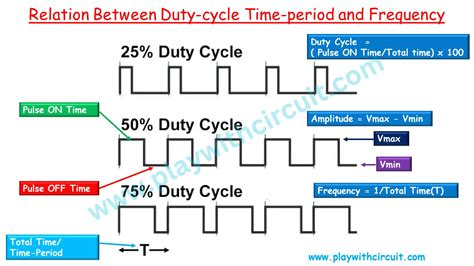
Fundamental Parameters for GATE:
-
Clock Period (): The time taken to complete one full cycle ():
-
Clock Frequency (): The number of clock cycles per second:
-
Duty Cycle: The percentage of total clock period during which the clock signal is HIGH ():
- Symmetrical Clock: A clock with a 50% duty cycle ().
- Example: A 100 MHz clock () with a 50% duty cycle has and .
-
Clock Triggering Regions (Level vs. Edge): Every clock period contains two voltage levels and two transition edges:
- HIGH Level (): Signal remains at logic . Level-triggered active-high latches remain transparent during this entire duration.
- LOW Level (): Signal remains at logic .
- Rising Edge (): The instantaneous low-to-high transition (). Positive edge-triggered flip-flops sample data at this exact instant.
- Falling Edge (): The instantaneous high-to-low transition (). Negative edge-triggered flip-flops sample data at this exact instant.
1.5 Triggering Classification: Latches vs. Flip-Flops (Core GATE Rule)
Understanding how triggering mechanisms are visually represented in circuit schematics is essential for solving GATE block diagram questions:
IMPORTANT
- LATCHES use LEVEL TRIGGERING: A latch is enabled and transparent for the entire duration (voltage level) that the clock or enable signal is held at logic (or logic ).
- FLIP-FLOPS use EDGE TRIGGERING: A flip-flop is non-transparent and samples inputs only at the split-second transition edge (rising or falling ) of the clock pulse.
How Schematic Symbols Represent Triggering Modes
In digital schematics, two distinct visual notation rules dictate how clock pins are drawn:
-
Presence of Dynamic Indicator ():
- No Triangle: Represents a Level-Triggered Latch.
- Triangle () inside the block: Represents an Edge-Triggered Flip-Flop (the triangle is called the Dynamic Indicator).
-
Presence of Inversion Bubble ():
- No Bubble: Active on Positive / High signal ( or Rising Edge ).
- Bubble () outside the block: Active on Negative / Low signal ( or Falling Edge ).
The 4 Clock Input Symbol Configurations
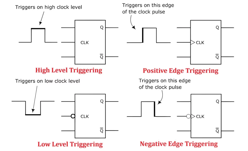
  1. Positive Level Latch      2. Negative Level Latch
     +--------------+             +--------------+
     |            Q |             |            Q |
CLK -|              |       CLK -o|              |
     |            Q'|             |            Q'|
     +--------------+             +--------------+
  (Active while CLK = 1)       (Active while CLK = 0)


  3. Positive Edge Flip-Flop   4. Negative Edge Flip-Flop
     +--------------+             +--------------+
     |            Q |             |            Q |
CLK ->|             |       CLK -o>|             |
     |            Q'|             |            Q'|
     +--------------+             +--------------+
  (Samples on 0 -> 1 Edge)     (Samples on 1 -> 0 Edge)
Summary Triggering & Symbol Matrix for GATE:
| Memory Element Type | Triggering Mechanism | Active Sampling Condition | Clock Pin Schematic Symbol |
|---|---|---|---|
| Positive (High) Level Latch | Level-Triggered | (High Voltage) | Plain pin labeled (No , No ) |
| Negative (Low) Level Latch | Level-Triggered | (Low Voltage) | Bubble () on pin (No ) |
| Positive Edge-Triggered Flip-Flop | Edge-Triggered | Rising Edge () () | Dynamic Triangle () inside pin |
| Negative Edge-Triggered Flip-Flop | Edge-Triggered | Falling Edge () () | Bubble + Triangle () on pin |
2. SR Latches (Set-Reset)
An SR Latch is the fundamental 1-bit memory element. It has two inputs: Set () and Reset (), and two complementary outputs: (normal output) and (inverted output).
2.1 SR NOR Latch (Active-High)
An active-high SR Latch is constructed using two cross-coupled NOR gates.
Circuit Schematic
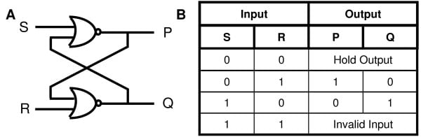
Truth Table (Active-High SR NOR Latch)
| Next State () | State Description | |||
|---|---|---|---|---|
| 0 | 0 | No Change / Memory (Hold) | ||
| 0 | 1 | 0 | 1 | Reset State () |
| 1 | 0 | 1 | 0 | Set State () |
| 1 | 1 | 0 | 0 | Forbidden / Invalid State () |
Detailed Operation Analysis:
- (Hold): NOR gate output with one 0 input equals the complement of the other input. The feedback retains the previously stored bit .
- (Reset): forces top NOR gate output . Then forces bottom NOR gate output .
- (Set): forces bottom NOR gate output . Then forces top NOR gate output .
- (Forbidden / Invalid): Both and force and . This violates the fundamental output rule (). Furthermore, if and transition simultaneously back to , the final state is unpredictable (race condition).
2.2 SR NAND Latch (Active-Low)
An active-low SR Latch is constructed using two cross-coupled NAND gates. The inputs are active-low, denoted as and (or and ).
Circuit Schematic
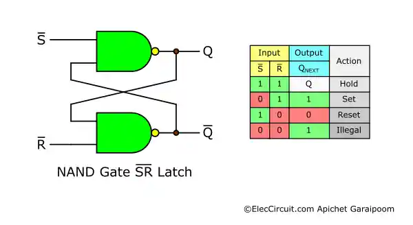
Truth Table (Active-Low SR NAND Latch)
| Next State () | State Description | |||
|---|---|---|---|---|
| 0 | 0 | 1 | 1 | Forbidden / Invalid State () |
| 0 | 1 | 1 | 0 | Set State () |
| 1 | 0 | 0 | 1 | Reset State () |
| 1 | 1 | No Change / Memory (Hold) |
IMPORTANT
Compare NOR vs NAND SR Latches carefully!
- For NOR Latch: Active-High ( sets, resets, holds, forbidden).
- For NAND Latch: Active-Low ( sets, resets, holds, forbidden).
2.3 Gated SR Latch (with Enable Pin)
To control when the SR Latch responds to inputs, two steering NAND gates and an Enable () pin are added to an active-low NAND latch.
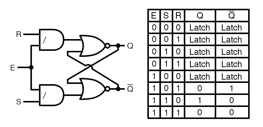
Functioning:
- When : Steering NAND gate outputs are forced to . The internal NAND latch sees Hold State (inputs and are ignored).
- When : Steering NAND gates invert and (), converting the circuit into an Active-High Gated SR Latch:
| State Description | ||||
|---|---|---|---|---|
| 0 | X | X | Disabled (Hold) | |
| 1 | 0 | 0 | Hold | |
| 1 | 0 | 1 | 0 | Reset |
| 1 | 1 | 0 | 1 | Set |
| 1 | 1 | 1 | Invalid | Forbidden () |
2.4 Characteristic Equation & Excitation Table
1. Characteristic Equation
Using a K-Map derived from the truth table (with as a constraint condition):
2. Excitation Table
The excitation table specifies the required inputs () needed to cause a desired state transition from present state to next state :
| Present State () | Next State () | Required | Required | Notes / Explanation |
|---|---|---|---|---|
| 0 | 0 | 0 | X | Can be Hold () or Reset () |
| 0 | 1 | 1 | 0 | Must Set () |
| 1 | 0 | 0 | 1 | Must Reset () |
| 1 | 1 | X | 0 | Can be Hold () or Set () |
3. D Latches (Data / Delay)
A D Latch (where D stands for Data or Delay) is designed to overcome the major disadvantage of an SR Latch: the invalid/forbidden state ().
3.1 Basic D Latch Concept
In an SR Latch, the forbidden state occurs when both and are simultaneously . To prevent this:
- We use a single input line .
- We connect directly to the Set input () and its inverse via a NOT gate to the Reset input ().
Since and are always exact complements, the condition is physically impossible.
3.2 Gated D Latch (Transparent Latch)
A Gated D Latch adds an Enable () signal to control when input is allowed to affect output .
Circuit Schematic
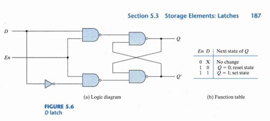
Truth Table (Gated D Latch)
| Enable () | Data () | Next State () | State Description | |
|---|---|---|---|---|
| 0 | X | Disabled / Hold (Remembers previous bit) | ||
| 1 | 0 | 0 | 1 | Reset () |
| 1 | 1 | 1 | 0 | Set () |
Key Intuition:
- When : The internal latch inputs are forced to (Hold mode). Data input is completely blocked.
- When : Output follows input directly (). This is why it is called a Transparent Latch!
3.3 Characteristic Equation & Excitation Table
1. Characteristic Equation
From the truth table of the Gated D Latch:
When enabled ():
2. Excitation Table (for )
The excitation table shows the input required to achieve a desired transition ():
| Present State () | Next State () | Required |
|---|---|---|
| 0 | 0 | 0 |
| 0 | 1 | 1 |
| 1 | 0 | 0 |
| 1 | 1 | 1 |
TIP
Notice how clean the D Latch excitation table is: Required simply equals the desired next state !
3.4 Level Transparency & Timing Parameters
1. Level Transparency Issue
While , the D Latch remains transparent. If input experiences noise, glitches, or multiple state transitions while , all those changes will propagate immediately to output .
2. Timing Parameters (GATE Favorites)
To guarantee reliable state storage, input must satisfy two timing constraints relative to the falling edge of Enable ():
- Setup Time (): The minimum time duration that input must remain stable before Enable transitions from to .
- Hold Time (): The minimum time duration that input must remain stable after Enable transitions from to .
WARNING
Violating or causes Metastability—the latch output enters an undefined intermediate voltage level between and for an unpredictable duration!
4. Edge-Triggered D Flip-Flops
4.1 Concept & Difference from D Latch
While a D Latch is level-sensitive and transparent whenever , an Edge-Triggered D Flip-Flop (Data / Delay Flip-Flop) samples the data input only at a split-second clock edge ( rising edge or falling edge).
- During the steady HIGH or LOW clock phase, the D Flip-Flop is completely non-transparent and ignores any variations at input .
- Physical Construction: Built either using Master-Slave D latches or 6-NAND gate edge-detector circuits.
Circuit Symbol
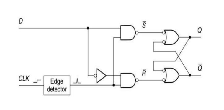
4.2 Truth Table & Symbol
Positive (Rising) Edge-Triggered D Flip-Flop
| Clock () | Data () | Next State () | State Description | |
|---|---|---|---|---|
| 0 | X | Hold (Clock steady LOW) | ||
| 1 | X | Hold (Clock steady HIGH) | ||
| X | Hold (Falling edge ignored) | |||
| 0 | 0 | 1 | Reset () | |
| 1 | 1 | 0 | Set () |
4.3 Characteristic Equation & Excitation Table
1. Characteristic Equation
For an edge-triggered D Flip-Flop at the sampling edge:
2. Excitation Table
The excitation table specifies the required input at the clock edge to achieve a desired transition ():
| Present State () | Next State () | Required |
|---|---|---|
| 0 | 0 | 0 |
| 0 | 1 | 1 |
| 1 | 0 | 0 |
| 1 | 1 | 1 |
5. T Flip-Flops (Toggle)
5.1 Concept & Circuit Realization
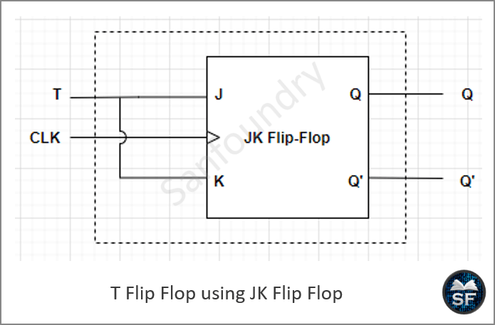
A T Flip-Flop (where T stands for Toggle) is a 1-input single-bit memory element designed specifically for state toggling and frequency division.
How to Build a T Flip-Flop:
- From a JK Flip-Flop: Tie inputs and together .
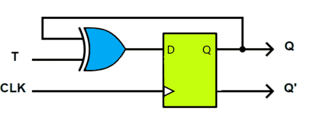
- From a D Flip-Flop: Feed back output through an XOR gate with input .
5.2 Truth Table & State Analysis
Positive Edge-Triggered T Flip-Flop
| Clock () | Toggle () | Next State () | State Description | |
|---|---|---|---|---|
| 0, 1 | X | Hold (Clock steady) | ||
| 0 | No Change / Hold () | |||
| 1 | Toggle () |
5.3 Characteristic Equation & Excitation Table
1. Characteristic Equation
From the truth table:
2. Excitation Table
The excitation table shows the input required to cause a state transition ():
| Present State () | Next State () | Required | Explanation |
|---|---|---|---|
| 0 | 0 | 0 | No state change |
| 0 | 1 | 1 | State toggles |
| 1 | 0 | 1 | State toggles |
| 1 | 1 | 0 | No state change |
TIP
Notice that for a T Flip-Flop: If present state and next state are different . If they are the same .
5.4 Frequency Division Property ()
When input is permanently tied HIGH (), the T Flip-Flop toggles its output on every active clock edge.
- Two active clock edges ( clock cycles) are required for output to complete one full period.
- Therefore, the output frequency is exactly half of the input clock frequency :
NOTE
Cascading T-flip-flops in series divides the input clock frequency by : This is the fundamental operating principle behind Asynchronous Binary Ripple Counters!
6. JK Flip-Flops & Race-Around Condition
6.1 Motivation & Circuit Logic
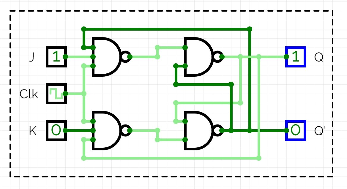
In an SR Latch/Flip-Flop, the input combination is invalid because it forces (or ).
The JK Flip-Flop (named after Jack Kilby) resolves this limitation by feeding back output lines and into steering NAND/AND gates at the inputs:
- acts as the Set input ().
- acts as the Reset input ().
Circuit Schematic
6.2 Truth Table & State Analysis
When and , the feedback forces the flip-flop to invert its current state—this is called Toggling ().
| Next State () | State Description | |||
|---|---|---|---|---|
| 0 | 0 | No Change / Memory (Hold) | ||
| 0 | 1 | 0 | 1 | Reset State () |
| 1 | 0 | 1 | 0 | Set State () |
| 1 | 1 | Toggle State () |
6.3 Characteristic Equation & Excitation Table
1. Characteristic Equation
Constructing a 3-variable K-Map for :
2. Excitation Table
The excitation table specifies the required inputs to achieve a desired state transition ():
| Present State () | Next State () | Required | Required | Explanation / Derivation |
|---|---|---|---|---|
| 0 | 0 | 0 | X | Can be Hold () or Reset () |
| 0 | 1 | 1 | X | Can be Set () or Toggle () |
| 1 | 0 | X | 1 | Can be Reset () or Toggle () |
| 1 | 1 | X | 0 | Can be Hold () or Set () |
TIP
Notice the symmetry of the JK excitation table!
6.4 The Race-Around Condition
The Race-Around Condition is a critical flaw that occurs in level-triggered JK Flip-Flops (or latches).
Conditions for race condition -
- Level triggered JK Flip-Flops
- i/p is and
- , clock pulse remains HIGH for a duration that is longer than the propagation delay
Definition & Mechanism
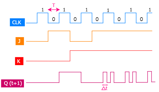
When and , the flip-flop is in Toggle mode. If the clock pulse remains HIGH () for a duration that is longer than the propagation delay of the flip-flop ():
- At , . Input causes to toggle to after delay .
- Since is still HIGH, this new output feeds back to the input, causing to toggle back to after another delay .
- continues toggling wildly () for as long as .
- At the end of , the final output state is unpredictable (depends on whether the number of toggles was even or odd)!
Conditions for Race-Around to Occur:
- and (Toggle mode).
- Level-triggered clock is HIGH ().
- Clock HIGH duration exceeds flip-flop propagation delay ().
Remedies to Prevent Race-Around:
- Reduce Clock Pulse Width: Make (hard to achieve in physical ICs because is extremely small, ~picoseconds).
- Use Edge Triggering: Sample data only at the instantaneous clock edge ( or ), so becomes effectively zero.
- Use Master-Slave Configuration: Use a Master-Slave JK Flip-Flop (the classic hardware solution).
7. Master-Slave Flip-Flops
7.1 Master-Slave Operating Principle
A Master-Slave Flip-Flop cascades two level-sensitive latches in series:
- Master Latch: Driven directly by the main clock signal .
- Slave Latch: Driven by the inverted clock signal (or inverter output).
          +--------------+             +--------------+
Inputs -->| Master Latch |--> Y (Qm) ->| Slave Latch  |--> Q (Output)
          | (Active CLK) |             | (Active ~CLK)|
          +--------------+             +--------------+
                 ^                            ^
                 |                            |
       CLK ------+------------------[NOT]-----+
Key Operating Property:
Since Master and Slave are driven by complementary clock signals, both latches are NEVER active at the same time!
- When : Master is enabled (samples inputs), Slave is disabled (locked).
- When : Master is disabled (locked), Slave is enabled (passes Master’s state to output ).
7.2 Master-Slave D Flip-Flop
A Master-Slave D Flip-Flop turns level-sensitive D-latches into a Negative Edge-Triggered () D Flip-Flop.
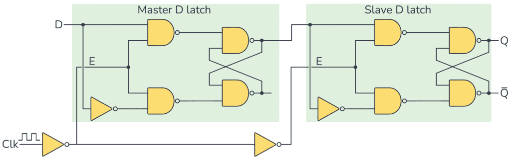
Sequence of Events across a Clock Cycle:
- While : Master latch is enabled and follows input (). Slave latch is disabled ( for Slave), so output remains unchanged.
- At Falling Edge ():
- Master latch becomes disabled, locking the instantaneous value of present right before the falling edge into intermediate node .
- Slave latch becomes enabled, passing node directly to final output .
- While : Master is locked, so changes at input cannot reach or .
Thus, the output updates only at the falling edge () of :
7.3 Master-Slave JK Flip-Flop
The Master-Slave JK Flip-Flop completely eliminates the Race-Around Condition.
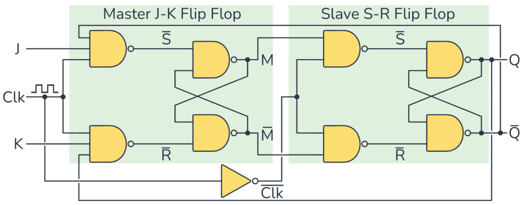
How Master-Slave Eliminates Race-Around:
- When and :
- Master receives feedback from Slave output . Since Master is enabled, it toggles once ().
- Because , the Slave is disabled (). Output cannot change while .
- Therefore, the feedback to the Master cannot change while , preventing multiple toggles!
- On the falling edge (), Master locks , and Slave passes to final output .
The output toggles exactly once per clock cycle, regardless of how long lasts!
8. Roadmap & Future Expansion (Registers & Counters)
This note will be continuously expanded as we study further topics in Sequential Circuits:
- Flip-Flop Conversions: Systematic method to convert any Flip-Flop type to type using excitation tables.
- Registers & Shift Registers: SISO, SIPO, PISO, PIPO, Universal Shift Register, Ring Counter, Johnson Counter.
- Synchronous & Asynchronous Counters: Ripple counters, Modulo- counters, state transition diagrams, and lock-out condition resolution.
9. GATE PYQ-Style Solved Questions
Q1) A cross-coupled NAND latch has inputs \bar{S} = 0 and \bar{R} = 1. What are the outputs Q and \bar{Q}?
Sol - Recall the NAND SR Latch active-low input rules:
- Inputs are and .
- Since (active low Set signal is triggered), the latch enters the Set state.
- Output and .
Q2) What happens to an active-high SR NOR latch if both inputs S = 1 and R = 1 are applied simultaneously, and then both inputs change to S = 0 and R = 0 at the exact same instant?
Sol -
- When and are applied to a NOR latch:
- Top NOR gate: .
- Bottom NOR gate: .
- Outputs become and (violating the complementary output property).
- When inputs simultaneously drop to :
- Both NOR gates see inputs and try to output at the same time.
- The final state depends on microscopic gate propagation delay differences. This creates an unpredictable race condition / metastable state.
Q3) A Gated D Latch has its Enable input E connected to a clock signal of frequency 1 MHz with a 50% duty cycle. If input D is held constant at 1, for how long in each clock cycle is the output Q transparent to input D?
Sol -
- Clock period .
- With a 50% duty cycle, the clock / Enable signal is HIGH () for half the period:
- Since a Gated D Latch is transparent whenever , output is transparent for 500 ns in each 1000 ns clock cycle.
Q4) A JK flip-flop has propagation delay t_{ff} = 10 ns. It is driven by a clock signal of frequency f = 20 MHz with a 50% duty cycle. If inputs are held at J = 1 and K = 1, will the race-around condition occur?
Sol -
- Calculate Clock Period :
- Calculate Clock HIGH pulse width (50% duty cycle):
- Compare with propagation delay :
- Since under , the output will toggle times during the single HIGH pulse Race-Around Condition WILL occur.
Q5) A cascade of 4 positive-edge-triggered T flip-flops, each with T = 1, is driven by a 16 MHz clock. What is the frequency of the output signal of the 4th flip-flop?
Sol -
- Recall the frequency division property of a T flip-flop with :
- Each T flip-flop divides input frequency by .
- For cascaded T flip-flops: